DOCUMENT
NO.
REV.NO
PAGE
STANDARD
NAME
SPECIFICATION FOR APPROVAL
00 6/10
4 .0 FUNCTIONAL DESCRIPTION
Input data from the host system is loaded into the module’s display buffer via the
serial data input channel. The internal timing and control system synchronizes the
signal and digit output signals to provide correct timing for the multiplexing
operation. A 16 x 64 bit programmable logic array (PLA) is provided for segment
decoding of the full upper-case ASCII character set. Input data from the host
system is loaded as a series of 8-bit data bytes clocked in on the high to low
transition of the clock.
Control and Character Data Bytes
The most significant bit (bit 7) is loaded first and is referred to as the control bit
(C-bit). If the C-bit of any byte is logical 1, the byte is a control data byte; if it is
logical 0, the byte is a character data byte. The functions and formats of control and
character data bytes are described in detail below.
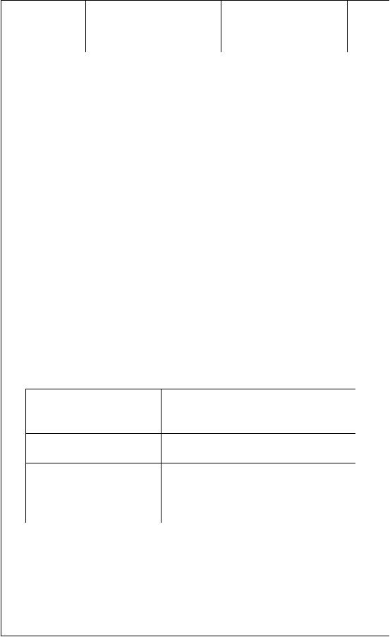
4.1 WRITING CONTROL DATA BYTES
When the C-bit of the loaded byte is logical 1, it is recognized as a control data
byte. See table below for the format and explanation of each.
8-BIT CONTROL
BYTE
7 6 5 4 3 2 1 0
FUNCTION
1 0 1 0 X X X X
Load Buffer Pointer
(position of character to be defined)
1 1 0 0 Y Y Y Y
Load Digit Counter
(number of characters to be displayed)
1 1 1 Z Z Z Z Z
Load Duty Cycle
(luminance level control)
Notes: 1. “XXXX” – 4 bit binary value of the digit position to be written to
2. “YYYY” – 4 bit binary value of the number of characters to be displayed
3. “ZZZZZ”– 5 bit binary va
lue divided by 31 times 100% equals
luminance level.
发布紧急采购,3分钟左右您将得到回复。
相关PDF资料
M0116SY-161MSAR1
MODULE VF CHAR 1X16 5MM
M0120SD-201MDBR1-1
MODULE VF CHAR 1X20 4.9MM
M0121LB-222LHAR2-I1
MODULE VF CHAR 1X21 14.5MM
M0216MD-162MDBR2-J
MODULE VF CHAR 2X16 9.22MM
M0216SD-162SDAR1
MODULE VF CHAR 2X16 4.34MM
M0216SD-162SDAR2-1
MODULE VF CHAR 2X16 5.34MM
M0216SD-162SDAR8
MODULE VF CHAR 2X16 5.34MM
M0220MD-202LDAR2
MODULE VF CHAR 2X20 10.5MM
相关代理商/技术参数
M0116SY-161MSAR1-S2C
功能描述:真空荧光显示器 - VFD VFD Dot Matrix 125.0 x 35.5 x 18.0
RoHS:否 制造商:Noritake 产品:Graphic Display Modules 字符计数 x 行: 模块大小 - 宽x高x厚:230 mm x 78 mm x 15 mm 观察区域 - 宽x高:166.25 mm x 41.45 mm 接口: 电压额定值:5 V 工作温度范围:- 40 C to + 85 C 封装:
M011AA002-01
功能描述:以太网模块 Micro 100 w/RJ45 Jck LEDS TTL pin hdr
RoHS:否 制造商:Lantronix 产品:Device Servers 数据速率:300 bps to 921.6 kbps, 10 Mbps, 100 Mbps 接口类型:Ethernet, Serial 工作电源电压:5 V to 15 V 工作电源电流:133 mA to 400 mA 最大工作温度:+ 70 C
M011U WAF
制造商:Fairchild Semiconductor Corporation 功能描述:
M012
制造商:Kemo Electronic 功能描述:Power Control 110Vac/1200 Va
M012021-00A
制造商:Teac 功能描述:ESCUTHEON;BLACK;FOR CD516E/KIT 制造商:Teac 功能描述:BLACK TRAY FOR CDW516EB02 - Bulk
M012021-02A
制造商:Teac 功能描述:PS/2 TRAY COVER - Bulk
M0120MD-201MDBR2-1
功能描述:真空荧光显示器 - VFD DIM=164.0x34.0x25.5 5 x 8 Dot RoHS:否 制造商:Noritake 产品:Graphic Display Modules 字符计数 x 行: 模块大小 - 宽x高x厚:230 mm x 78 mm x 15 mm 观察区域 - 宽x高:166.25 mm x 41.45 mm 接口: 电压额定值:5 V 工作温度范围:- 40 C to + 85 C 封装:
M0120SD-201MDBR1-1
功能描述:真空荧光显示器 - VFD DIM=150.0x32.0x25.5 5 x 7 Dot RoHS:否 制造商:Noritake 产品:Graphic Display Modules 字符计数 x 行: 模块大小 - 宽x高x厚:230 mm x 78 mm x 15 mm 观察区域 - 宽x高:166.25 mm x 41.45 mm 接口: 电压额定值:5 V 工作温度范围:- 40 C to + 85 C 封装:
